You are here: CBM Wiki>Public Web>PublicNxyter (2016-02-15, PierreAlainLoizeau)Edit Attach
n-XYTER - Read-out ASIC for High Resolution Time and Amplitude Measurements
Introduction
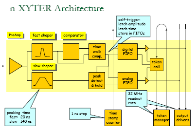
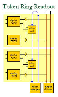
The n-XYTER ASIC was developed in context of the EU-FP6 Integrated Infrastructure Initiative NMI3 in the Joint Research Activity DETNI as the common read-out solution for three different, solid converter based neutron counting area detectors. Because of the the statistical, non-triggerable nature of neutron data to be processed, the internal architecture of the chip is self triggered and data driven. It integrates 128 channels with low noise preamplifiers and shapers. Each channel has two different shapers with distinct time constants, one optimized for timing resolution, the other one optimized for energy (pulse height) resolution. A peak detector connected to the slower shaper allows for the application of a spectroscopic amplitude measurement. An internal time stamp generator provides the temporal reference that may be employed to identify time coincidences of signals on different detector channels and thus correlate their spatial point of origin. For testability and calibration purposes, a charge injector with adjustable pulse height was implemented. The bias settings and various other parameters can be controlled via a standard I2C -interface.Key Features
- mixed signal chip
- process: AMS 0.35 μm CMOS
- 128 channels
- 1 test channel with analogue diagnostic output
- architecture for AC-coupling, employable for positive and negative signals
- self triggered, data driven de-randomizing, sparcifying readout at 32 MHz
- digital time stamp output
- analogue peak hight output
- maximum data loss at 32 MHz average input rate over 16 μs: 4%
- analogue pile-up registry
- programmable dead time
- local threshold adjustment
- Dynamic Range: 120000 e
- Shaping time and noise performance:
- 18 ns fast shaper at 30 pF input, 850 enc for positive signals, 1000 enc for negative signals
- 140 ns slow shaper at 30 pF input, 600 enc
- Timing resolution ~ 2-3 ns, time stamp resolution 1 ns
Documentation
- n-XYTER Reference Manual, describes in detail electrical specifications, operating conditions and port definitions of the readout chip n-XYTER 1.0.
- Version 1.50 (Draft) of 15.12.2009 (Improvement in the documentation of time-stamp generation)
- Version 1.40 (Draft) of 25.05.2009 (Improvements on strategies for finding Vcm settings and help for compensation of temp co.)
- Version 1.30 (Draft) of 29.03.2009
- Version 1.30 (Draft) of 29.07.2008
- Version 1.30 (Draft) of 24.07.2008
- Version 0.90 of 28.02.2008
Papers and Presentations
- C.J. Schmidt et al., Test results on the n-XYTER ASIC, a self triggered, sparcifying readout ASIC, Topical Workshop on Electronics for Particle Physics 2007, TWEPP-07, 3-7 September 2007, Prague
- A.S. Brogna et al., N-XYTER, a CMOS read-out ASIC for high resolution time and amplitude measurements on high rate multi-channel counting mode neutron detectors, Nucl. Instrum. Methods A 568 (2006) 301308
User changes from nXYTER 1 to nXYTER 2.0
The only change on the user side is that the v{bfb, biasF, biasS, biasS2} i2c registers functionality are replaced by externally set voltages. On the CBM STS FEB-E and FEB-F, these voltages are set by a 12 bins DAC between GND and 2.4V. Therefore the scan of vbiasS which was done on the previous nXYTER to find the proper operating point using the FEB ADC values is replaced by a scan of the DAC codes for the corresponding external voltage. On the FEB-E, the relation between DAC code and external voltage is the following:V (mV) = DAC(bin) * 2440 / 65535The relation between a monitoring voltage and its measured ADC code is:
V (mV) = ADC(bin) * 3300 / 1024Using the FEB-E #11, following relations were found between the DAC codes for the Vr, Vf, Vs and Vs2 external voltages, the Vfast and Vslow nXYTER shaper monitoring voltages and the FEB ADC median value:
Default values for the DAC (in FEB-E with FW v0.992) are:
Vr = 0x3a70, Vcf = 0x388c, Vcs = 0x3a55, Vcs2 = 0x3a55, corresponding to
Vr = 556 mV, Vcf = 538 mV, Vcs = 555 mV, Vcs2 = 555 mV

Vfast almost linear as function of the external voltages in the following bounds (all other voltages set to default values):
Vref DAC in [13500, 18000] bin ([503, 670] mV)
Vf   DAC in [12000, 18000] bin ([447, 670] mV)
Vs   DAC in [    0, 65535] bin ([0, 2440] mV)
Vs2  DAC in [    0, 65535] bin ([0, 2440] mV)

Vslow almost linear as function of the external voltages in the following bounds (all other voltages set to default values):
Vref DAC in [13750, 16500] bin ([512, 614] mV)
Vf   DAC in [    0, 65535] bin ([0, 2440] mV)
Vs   DAC in [13500, 16500] bin ([503, 614] mV)
Vs2  DAC in [10000, 23500] bin ([372, 875] mV)

Formula for Vfast is approximately:
Vfast =    58 + 0.057319 * Vref + -0.049384 * Vbiasf + 0.000000 * VbiasS + -0.000000 * VbiasS2

Formula for Vslow is approximately:
Vslow =   523 + 0.133591 * Vref + 0.000000 * Vbiasf + -0.124052 * VbiasS + -0.021365 * VbiasS2

=> Parameters for FEB ADC as function of Vslow in range 250 to 335
 FEB ADC = 2873 + Vslow * -8.12

=> Parameters for FEB ADC as function of Vslow in range 347 to 640
 FEB ADC = 7707 + Vslow * -10.71

The following sets of parameters leaded to reasonable FEB ADC median values (around 2000-2500 ADC codes) with FEB-E:
Vr = 0x3a70, Vcf = 0x388c, Vcs = 0x348a, Vcs2 = 0x3a55, corresponding to
Vr = 556 mV, Vcf = 538 mV, Vcs = 500 mV, Vcs2 = 555 mV
with Vfast  657 mV (Adc code:  204)  Vslow 1688 mV (Adc code:  524)
!!! Vs is then at the lower edge of the almost linear range for Vslow !!!

Vr = 0x3f00, Vcf = 0x388c, Vcs = 0x3a55, Vcs2 = 0x3a55, corresponding to
Vr = 600 mV, Vcf = 538 mV, Vcs = 555 mV, Vcs2 = 555 mV
with Vfast  886 mV (Adc code:  275)  Vslow 1646 mV (Adc code:  511)
-- WalterFJMueller - 30 Apr 2008
| I | Attachment | Action | Size | Date | Who | Comment |
|---|---|---|---|---|---|---|
| |
nXYTER.pdf | manage | 2 MB | 2009-12-15 - 17:06 | UnknownUser | nXYTER Reference Manual V1.5, 15.12.2009 |
Edit | Attach | Print version | History: r16 < r15 < r14 < r13 | Backlinks | View wiki text | Edit wiki text | More topic actions
Topic revision: r16 - 2016-02-15, PierreAlainLoizeau
 Copyright © by the contributing authors. All material on this collaboration platform is the property of the contributing authors.
 Ideas, requests, problems regarding CBM Wiki? Send feedback
Imprint (in German)
Privacy Policy (in German)

 alt="n-XYTER Architecture"/>
  alt="n-XYTER Architecture"/>


